Key Takeaways
- Broadcom reported $16.7B of AI semiconductor revenue in fiscal Q3 2026, up 221% YoY, and guided to roughly $115B in fiscal 2027 and $230B in fiscal 2028 — a scale that makes custom accelerators a core part of hyperscaler infrastructure rather than a side experiment.
- Custom AI silicon does not automatically reduce Nvidia’s relevance. Nvidia is responding with NVLink Fusion, NVHBM, and rack-architecture control, allowing it to retain the value of interconnect, memory integration, and software even as some accelerator silicon moves to hyperscaler XPUs.
- HBM demand may broaden rather than weaken. TrendForce expects global HBM consumption to rise by more than 70% in 2026, driven by Nvidia, AMD, Google TPU, and AWS Trainium — all of which are moving toward newer HBM generations.
- Networking becomes more valuable as compute becomes more diverse. Broadcom is positioning Tomahawk 6 (102.4 Tbps) and Ethernet as both a scale-out and a scale-up fabric, while tripling EML, CW laser, VCSEL, and indium-phosphide capacity in the U.S. and Singapore.
- Broadcom’s custom-silicon moat is not absolute. Google has expanded its custom-silicon relationship with Marvell through a $12.2B warrant structure, signaling that hyperscalers will multi-source rather than depend on a single supplier.
- The competitive unit is shifting from individual accelerators to the full AI factory. HBM, advanced packaging, networking, optics, power, and the data-center shell become the more durable shared bottlenecks, and Broadcom’s own outlook is gated by whether that surrounding infrastructure can be built fast enough.
Broadcom’s custom accelerators are moving into gigawatt-scale deployments. The bigger investment question is what happens to the AI infrastructure value pool when compute is no longer built around GPUs alone.
For most of the AI boom, investors could simplify the infrastructure trade into one assumption: more AI spending meant more Nvidia GPUs.
That shortcut is becoming less useful.
Broadcom reported $16.7 billion of AI semiconductor revenue in fiscal Q3 2026, up 221% year over year and 54% sequentially, and expects that figure to rise to $21.7 billion in Q4. The more important number sits further out. Broadcom now expects AI chip revenue of roughly $115 billion in fiscal 2027 and $230 billion in fiscal 2028. (investors.broadcom.com)
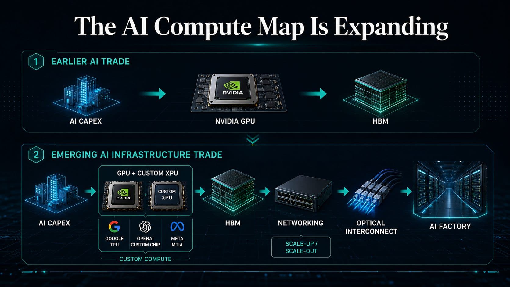
Those numbers are large enough to change how the AI compute market should be modeled. Custom accelerators are no longer a collection of experimental projects sitting beside the GPU market. Google, OpenAI, Meta, Anthropic and other hyperscale customers are building multigeneration custom-compute roadmaps measured in gigawatts, while Broadcom is supplying not only the accelerator silicon but increasingly the networking and connectivity around it. (investors.broadcom.com)
That does not mean Nvidia is about to lose the AI market. It means the AI infrastructure value pool is becoming more distributed.
The next phase is increasingly about custom compute + HBM + scale-up networking + scale-out networking + optics + advanced packaging, rather than GPUs alone.
Custom AI accelerators are moving from experiments to infrastructure
Hyperscalers have designed their own AI chips for years. Google has TPU, AWS has Trainium, Meta has MTIA, Microsoft has Maia. What remained uncertain was whether these programs would stay focused on a narrow set of internal workloads or become large enough to materially change how AI capital spending is allocated.
Broadcom’s current customer commitments suggest that threshold is being crossed.
In April, Broadcom disclosed a long-term agreement with Google to develop and supply future TPU generations, alongside a supply-assurance agreement covering networking and other components for next-generation AI racks through as late as 2031. The same filing said Anthropic would gain access through Broadcom to about 3.5 gigawatts of next-generation TPU-based compute beginning in 2027. (sec.gov)
OpenAI has gone further by designing its own accelerator with Broadcom. The first processor, Jalapeño, was built specifically around LLM inference and moved from design to manufacturing tape-out in nine months. OpenAI and Broadcom describe it as the first product in a multigeneration compute platform that will be deployed at gigawatt scale. (openai.com)
Broadcom has also described multigigawatt deployment plans with Meta and other customers. The exact timing will depend on whether data centers, power, substrates, HBM and other physical infrastructure are ready, but that itself is revealing. The bottleneck is no longer whether customers want custom silicon. It is increasingly whether the surrounding infrastructure can be built quickly enough to absorb it.
That is a very different industry from the one investors were looking at two years ago.
Why hyperscalers increasingly want their own AI chips
The economics become more compelling as workloads become larger and more predictable.
GPUs are powerful because they are flexible. Nvidia offers a mature software stack, broad model support, rapid deployment and a huge developer ecosystem. Those advantages matter enormously when architectures, training techniques and workloads keep changing.
A hyperscaler faces a different optimization problem once a workload reaches sufficient scale.
If Google, Meta or OpenAI knows that the same class of inference workload will consume gigawatts of compute for years, a custom chip can sacrifice some generality in exchange for better performance per watt, tighter integration with its software stack and lower cost per token.
OpenAI says early testing of Jalapeño shows performance per watt materially above current state-of-the-art systems for its target workload. That is a company claim rather than an industry-wide benchmark, but it illustrates why custom silicon becomes economically attractive when deployment moves from thousands of chips to entire gigawatt-scale campuses. (openai.com)
Industry data point in the same direction. TrendForce expects custom ASIC deployment to keep expanding as North American cloud providers push more internally designed AI infrastructure, even while Nvidia remains the dominant supplier of general-purpose AI acceleration. (trendforce.com)
The implication is more subtle than “ASIC beats GPU.”
Nvidia can continue growing rapidly while its share of incremental AI compute gradually declines.
That distinction matters much more for investors.
Custom silicon does not automatically mean less Nvidia
Nvidia is already adapting to this architecture shift.
NVLink Fusion allows hyperscalers and custom-chip designers to connect their own XPUs into Nvidia’s scale-up fabric and rack architecture rather than building an entire AI system from scratch. Marvell, MediaTek and other custom-silicon partners can use Nvidia interconnect technology while still supplying non-Nvidia accelerators. (nvidianews.nvidia.com)
That strategy effectively says:
custom accelerators can exist inside the Nvidia ecosystem.
Nvidia can therefore lose part of the accelerator silicon opportunity while retaining value in interconnect, networking, rack architecture, memory integration and software.
Its recent expansion of NVLink Fusion into NVHBM pushes that logic further. NVHBM moves more memory-controller functionality into a customized HBM base die and is designed to increase bandwidth while lowering HBM power and freeing compute-die area. Nvidia says the design can deliver up to 30% more bandwidth per stack and roughly 15% lower HBM power than standard HBM4E. (blogs.nvidia.com)
This is why I would not frame Broadcom’s growth as a simple transfer of value from Nvidia to Broadcom.
AI infrastructure is becoming more heterogeneous, and Nvidia is trying to own the common architecture connecting that heterogeneous compute.
Custom AI chips may increase the HBM bottleneck rather than weaken it
This is one of the most important second-order effects.
A custom accelerator still needs memory.
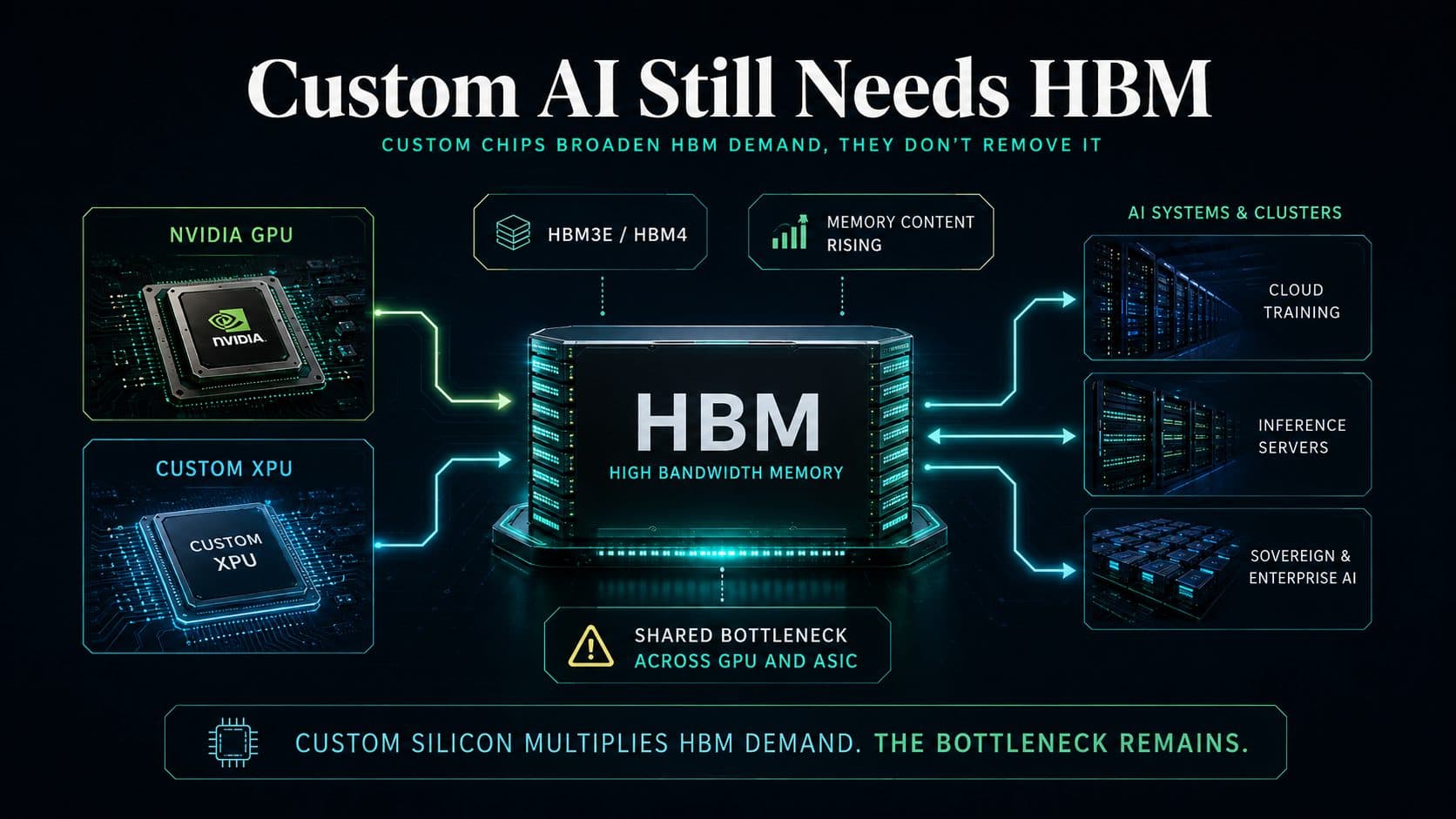
Google TPU, AWS Trainium and other high-end AI ASICs are increasingly moving toward newer HBM generations. TrendForce expects global HBM consumption to rise by more than 70% in 2026, driven not only by Nvidia and AMD accelerators but also by Google TPU and AWS Trainium adopting HBM3E. (trendforce.com)
That means the rise of custom silicon does not necessarily reduce the memory opportunity.
It can broaden it.
The older model was approximately:
Nvidia GPU growth → HBM growth.
The emerging model looks more like:
Nvidia GPU growth + custom XPU growth → HBM growth.
If hyperscalers substitute some Nvidia units with their own accelerators but deploy more total compute because custom silicon lowers cost per token, aggregate HBM demand can still rise.
That is why the Broadcom story fits directly into the memory thesis rather than sitting outside it. (For a deeper read on how the broader HBM cycle is being validated and where the 2027 risk shifts from demand to supply, see Is HBM Demand Really This Strong? Testing the AI Memory Boom Against Orders, Utilization, and 2027 Supply. For a foundational comparison of HBM and conventional DDR5, see HBM vs DDR5: What’s the Difference—and Why AI Needs Both.)
The key memory question becomes less about which accelerator vendor wins and more about how much HBM content per accelerator continues to increase across both GPU and ASIC platforms.
Networking becomes more important as compute becomes more diverse
Broadcom may be especially well positioned because it sells into both sides of this shift.
A custom accelerator can reduce silicon cost for a specific workload. It does not reduce the need to connect tens of thousands of accelerators together. If cheaper compute allows a hyperscaler to deploy more XPUs, networking demand can rise with it.
Broadcom is already seeing that effect. Its management says AI networking is expected to grow at roughly the same pace as XPUs over the coming years. (earningscalls.dev)
Tomahawk 6 shows why.
The 102.4 Tbps switch can connect 512 XPUs in a single scale-up domain, while a two-tier scale-out network can support more than 100,000 accelerators. Broadcom is positioning Ethernet not only as a scale-out fabric between racks but increasingly as a scale-up fabric inside AI systems. (investors.broadcom.com)
That changes the economics of the AI stack.
If compute becomes more fragmented across Nvidia GPUs, Google TPUs, OpenAI processors, Meta MTIAs and other XPUs, the fabric connecting all of those systems becomes more valuable rather than less.
The competitive unit is gradually moving from the individual accelerator toward the entire AI factory.
The next physical bottleneck may move further into optics
Broadcom’s latest earnings call also contained a useful signal for the optical supply chain.
Management said it is more than tripling year-over-year capacity across EML, CW laser, VCSEL and indium-phosphide manufacturing in the United States and Singapore, with further expansion planned over the next two years. Hock Tan said demand for EML and CW lasers is currently running well ahead of industry supply. (benzinga.com)
That deserves more attention than it received.
As AI clusters grow, every additional accelerator increases communication requirements. Faster SerDes eventually pushes more links beyond the practical reach or power envelope of copper, increasing the role of optical interconnect.
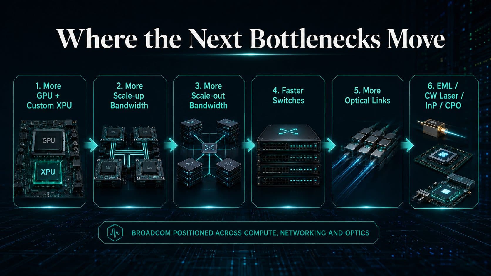
The chain becomes:
custom XPUs and GPUs
→ more scale-up bandwidth
→ more scale-out bandwidth
→ faster switches
→ more optical links
→ more EML, CW lasers, silicon photonics and eventually CPO.
Broadcom’s co-packaged optics roadmap is designed around that problem. The company says its CPO architecture can deliver more than 3.5× lower power consumption and about 40% lower optics cost per bit compared with conventional approaches. (broadcom.com)
This is also why Broadcom’s InP expansion matters for the broader AI optical thesis. (For the deep dive on the indium-phosphide and AI optical bottleneck dynamic, see AXTI: The AI Optical Bottleneck Is Real. But Can AXT Capture the Value?.)
It is not evidence that every external indium-phosphide substrate supplier will benefit equally. Broadcom is expanding some of its own device capacity, and the eventual supplier economics still depend on procurement, qualification and capacity agreements.
What it does confirm is the physical demand underneath the theme: AI networking is consuming enough optical capacity that one of the industry’s largest suppliers is rapidly expanding its own laser manufacturing footprint.
Broadcom does not have a permanent custom-silicon monopoly either
There is an important counterpoint.
The rise of custom AI chips does not guarantee that Broadcom captures all of the economics.
Google recently expanded its custom-silicon relationship with Marvell, granting the company a warrant structure worth up to $12.2 billion if business milestones are met. Reuters reported that the agreement could generate as much as $120 billion of revenue for Marvell through fiscal 2033. (reuters.com)
That should not automatically be interpreted as Google replacing Broadcom. Broadcom has a long-term TPU agreement with Google through the next generation of systems, and analysts have generally viewed Marvell as additional sourcing rather than an immediate displacement. (sec.gov)
But it does show how hyperscalers behave once a strategic component becomes important.
They multi-source.
The same dynamic exists in HBM. SK Hynix, Samsung and Micron operate behind a very high industry barrier, but customers still try to maintain multiple qualified suppliers.
Broadcom’s custom-silicon moat therefore comes from the breadth of its capabilities—SerDes, chip implementation, networking, packaging, optics and production execution—not from customers having no alternative.
That is an important distinction when thinking about long-term margins.
AI compute is becoming a systems competition
Broadcom’s $115 billion AI forecast matters because it provides operating evidence that custom compute has reached a scale where it can influence the structure of the AI infrastructure market.
But the biggest change is not simply that Broadcom sells more custom accelerators.
The competitive unit itself is changing.
Hyperscalers increasingly optimize:
cost per token, performance per watt, utilization and time to deployment
across an entire system rather than choosing the “best chip” in isolation. Nvidia has responded by expanding from GPUs into rack architecture, networking and custom-XPU integration. Broadcom is combining custom silicon with Ethernet networking and optics. Memory suppliers are moving deeper into logic, packaging and co-design.
That makes the shared physical bottlenecks more important.
Regardless of whether the accelerator is a GPU, TPU, MTIA or another XPU, the system still needs HBM, leading-edge wafers, substrates, advanced packaging, networking, optics, power and a data-center shell.
Broadcom itself has acknowledged that its revenue outlook depends on those constraints. Management has said demand can exceed the revenue it has guided because actual deployment still depends on supply availability and the pace at which customer infrastructure comes online. (reuters.com)
That is the part of the custom-chip boom I find more important than the Nvidia-versus-Broadcom framing.
Custom AI silicon can diversify compute.
It may actually make the shared bottlenecks around compute more valuable.
What would confirm this thesis next?
The next evidence should come from operating variables rather than more announcements that a hyperscaler is “designing its own chip.”
Broadcom’s custom-XPU revenue needs to keep scaling toward its 2027 and 2028 targets, and the Google, OpenAI, Anthropic and Meta deployments need to translate from gigawatt commitments into functioning AI capacity. Marvell’s progress with Google will show whether custom-silicon economics become concentrated in Broadcom or spread across a broader supplier base. (reuters.com)
At the infrastructure layer, I would watch whether HBM availability remains tight as ASIC shipments expand, whether AI networking continues to grow alongside custom compute, and whether Broadcom’s aggressive InP and laser-capacity expansion is absorbed without creating excess supply.
Those signals will tell us where the economic rent is actually accumulating.
Broadcom has already answered one question: custom AI chips are large enough to be a core part of hyperscaler infrastructure.
The harder and more valuable question now is which parts of the stack remain difficult to replicate as compute becomes increasingly custom.
For investors following AI infrastructure, that may matter more than the eventual GPU-versus-ASIC market-share number.
Sources
| No. | Source | Publisher | Date | Type | What it supports |
|---|---|---|---|---|---|
| 1 | Broadcom Q3 FY2026 earnings release and 8-K filing | Broadcom Investor Relations | 2026-09 | Company IR | $16.7B AI semiconductor revenue (Q3 FY2026), 221% YoY, 54% sequential; $21.7B Q4 FY2026 AI outlook; $115B FY2027 and $230B FY2028 AI chip forecasts; Tomahawk 6 102.4 Tbps switch. |
| 2 | OpenAI and Broadcom Jalapeño LLM-optimized inference processor | OpenAI / Broadcom | 2026 | Company IR | Jalapeño inference chip design-to-tape-out in 9 months, gigawatt-scale deployment roadmap, performance per watt commentary. |
| 3 | Broadcom 8-K filing (Google TPU and Anthropic compute) | U.S. Securities and Exchange Commission | 2026-04 | SEC | Long-term TPU development and supply agreement with Google, supply-assurance agreement through 2031, Anthropic access to ~3.5 GW of next-generation TPU-based compute from 2027. |
| 4 | Nvidia NVLink Fusion semi-custom AI infrastructure partner ecosystem | Nvidia | 2026 | Company IR | NVLink Fusion partner ecosystem (Marvell, MediaTek, custom-silicon partners), Nvidia interconnect strategy for heterogeneous compute. |
| 5 | Nvidia NVLink Fusion NVHBM custom high-bandwidth memory | Nvidia Blog | 2026 | Company IR | NVHBM architecture, +30% bandwidth per stack, ~15% lower HBM power vs standard HBM4E. |
| 6 | TrendForce: HBM and the memory wall | TrendForce | 2026 | Research | Global HBM consumption +70% in 2026 forecast, HBM3E adoption by Google TPU and AWS Trainium. |
| 7 | TrendForce: North American custom ASIC expansion | TrendForce | 2026-10 | Research | Custom ASIC deployment outlook, North American hyperscaler custom-silicon roadmap. |
| 8 | Broadcom now shipping world's first 102.4 Tbps switch | Broadcom Investor Relations | 2026 | Company IR | Tomahawk 6 102.4 Tbps, 512-XPU scale-up, 100,000+ accelerator two-tier scale-out. |
| 9 | Broadcom Q3 2026 earnings call transcript | Benzinga / Broadcom | 2026-09-02 | Company IR | Hock Tan commentary on EML, CW laser, VCSEL, indium phosphide capacity tripling, demand running ahead of industry supply. |
| 10 | Broadcom co-packaged optics (CPO) architecture | Broadcom | 2026 | Company IR | CPO architecture, 3.5× lower power and ~40% lower optics cost per bit vs conventional approaches. |
| 11 | Marvell $12.2B stock warrant for Google custom chip deal | Reuters | 2026-08-19 | Reputable financial media | Marvell-Google custom-silicon warrant structure, $120B potential revenue through FY2033, multi-source custom-silicon dynamic. |
| 12 | Broadcom forecasts quarterly revenue below estimates | Reuters | 2026-09-02 | Reputable financial media | Broadcom management acknowledging revenue upside depends on data-center, power, substrate, HBM, and packaging availability. |
Broadcom figures, customer commitments, and forward guidance are taken directly from Broadcom's own Q3 FY2026 earnings release, 8-K filing, and earnings call. Nvidia, Marvell, TrendForce, and Reuters reporting are used for product roadmaps, custom-silicon economics, HBM and ASIC market data. All forward-looking statements about gigawatt-scale custom compute, NVLink Fusion, HBM3E/HBM4, Tomahawk 6 networking, EML/CW laser/Indium Phosphide capacity, and CPO economics are subject to each company's own risk factors and disclosures.
Related Reading
Is HBM Demand Really This Strong? Testing the AI Memory Boom Against Orders, Utilization, and 2027 Supply
AI server orders, cloud utilization, and HBM contracts all point to real demand. The harder question for 2027 is whether high prices and new qualified supply begin to change the cycle.
HBM vs DDR5: What’s the Difference—and Why AI Needs Both
HBM supplies extreme bandwidth to AI accelerators, while DDR5 provides larger pools of system memory. Understanding the difference is essential for analyzing AI infrastructure and memory stocks.
AXTI: The AI Optical Bottleneck Is Real. But Can AXT Capture the Value?
Public research has accelerated the discovery of AXT’s strategic position in indium phosphide. The investment outcome now depends on whether operating economics can catch up with expectations already embedded in the stock.

Sivers Semiconductors (SIVE): When Does an AI Photonics Story Become a Business?
The market is already pricing a future in co-packaged optics, external laser sources and InP manufacturing. The harder question is whether qualification, capacity, yield and customer orders can turn that future into per-share cash flow.
NVIDIA’s Next Bottleneck Isn’t GPUs. It’s Data Movement.
Why AI factories are moving from copper to optical connectivity — and which suppliers deserve deeper research
Invest better with thoughtful research.
Join readers who receive our best ideas and insights straight to their inbox.
Disclosure
This article is for research and education only. It is not investment advice.
Comments